Scanning tunneling microscopy (STM) is a real-space imaging technique, that can produce topographic images of a surface with atomic resolution in all three dimensions, belongs to an expanding family of instruments commonly called Scanning probe microscope (SPM). The scanning tunneling microscope was invented by two scientists Gerd Binning and Heinrich Rohrer in 1981.
Principle of scanning tunneling microscopy
Scanning tunneling microscopy works in the principle of quantum mechanical electron tunneling. If a bias voltage is applied between two metals separated by an insulating barrier or medium of thickness less than 1nm, there is a finite probability of flow of tunneling current. i.e electrons can tunnel across the barrier.
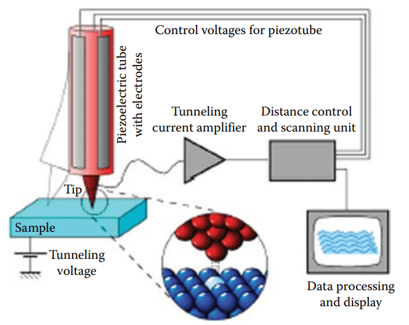
A scanning tunneling microscope uses an atomically sharp tip, usually made of tungsten or Platinum-Iridium. When the tip is within a few Å of the sample’s surface and a bias voltage is applied between the sample and the tip, quantum mechanical tunneling takes place across the gap. It is called the tunneling current.
Tunneling current depends exponentially on the separation d between the tip and the sample and linearly on the local density of states. The quality of STM images depends critically on the mechanical and electronic structure of the tip.
In a typical experiment, a conductive tip made up of tungsten(W) or Pt-Ir mounted to a piezoelectric material is scanned very close to a conductive sample by applying a bias voltage in the range of 0.01-1V. A feedback loop operates on the scanner to maintain a constant separation between the tip and the sample. Monitoring the position of the scanner provides a precise measurement of the tip’s position in three dimensions.
Modes of operation
The STM microscope can be operated in two modes.
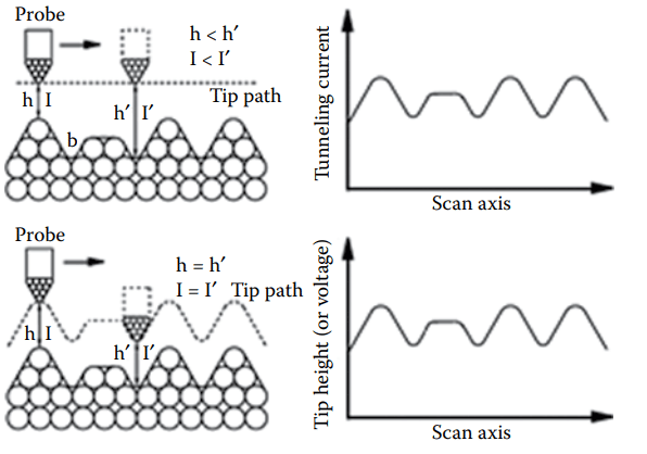
- Constant current mode: In this mode, the current is made constant during scanning by changing the distance between the tip and surface.
- Constant height mode: In this mode, tip height is made constant and tunneling current at every step of scanning is measured.
Sample specification in Scanning tunneling microscopy
Not all samples can be characterized by this technique. Some important sample specifications are listed below:
- STM requires a conducting surface to establish the tunneling current.
- Requires rigid solid surface otherwise, the probes will deform the surface while scanning.
- It limits the analysis of the conductive and semiconductive thin samples only ( not for insulators.)
Instrumentation of scanning tunneling microscopy
A typical STM microscope consists of major three components.
- Probe: It is made of tungsten or platinum-iridium alloy.
- Piezoelectric tube ( PZT)
- Feedback units
Application of Scanning tunneling microscopy
Important information can be obtained by using this technique.
- Shape, size, and organizations of individual particles or molecules along with the topographical information can be determined.
- The topographical information obtained from the analysis of STM helps to characterize the surface roughness of the samples.
- Electronic information of various conducting surfaces can be determined.
- A large charge in tunneling current is an indicator of the presence of atoms of different types or the presence of contaminants like absorbed gas.
STM youtube video
References
- C. R. Brundle, C. K. Evans, Jr., S. Wilson and L. E. Fitzpatrick (eds), Encyclopedia of Materials Characterization: Surfaces, Interfaces, Thin Films, Butxetworch-Heinemann, Reed Publishing (USA) Inc., 1992