Table of Contents
ToggleScanning electron microscopy principle, instrumentation, application, and its limitations have been discussed in this post. Scanning electron microscopy (SEM) is one of the most significant tools for characterizing material morphology on a nanometer to the atomic scale. This technique was developed by Manfred von Ardenne.
Scanning electron microscopy principle
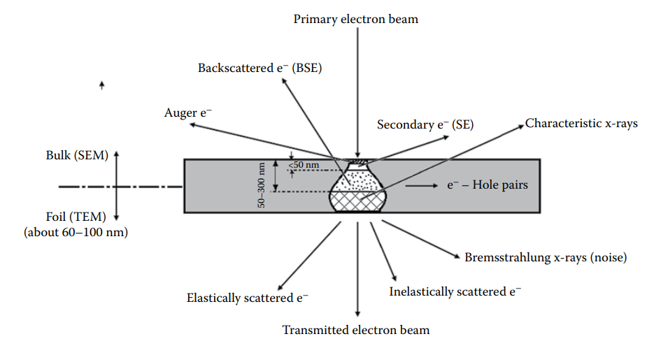
In scanning electron microscopy, a beam of electrons that are accelerated to kinetic energy in the range of 500 eV- 50 KeV is focused into a fine probe that is scanned over the surface of the specimen. As the electrons penetrate the surface, a number of interactions occur that can result in the emission of electrons or photons from or through the surface.
A fraction of the electrons emitted can be collected by appropriate detectors and the output can be modulated by the brightness of a cathode ray tube (CRT) whose x-ray and y-inputs are driven in synchronism with x-y voltages rastering the electron beam. In this way, an image is produced on the CRT. Every point that the beam strikes on the samples are applied directly onto a corresponding point on the screen.
The principle image produced in the SEM due to electron-matter interactions is of three types.
- Secondary electrons image
- Backscattered elastic imaging
- Elemental x-ray imaging( Energy dispersive x-ray/EDS/EDX)

Secondary electrons image
When a high-energy primary electron interacts with an atom, it undergoes either inelastic scattering with atomic electrons or elastic scattering with the atomic nucleus. In an inelastic collision with an electron, some amount of energy is transferred to the other electron. If the energy transfer is very small, the emitted electrons will probably not have enough energy to exit the surface. If the energy transferred exceeds the work function of the material the emitted electron can exist in the solid. To get an image, the incident electron beam is raster-scanned, and secondary electron beams are detected at each position.
When the energy of the emitted electron is less than about 50eV, by convection it is referred to as a secondary electron (SE) or simply a secondary. Most of the emitted secondaries are produced within the first few nm of the surface. Secondaries produced much deeper in the material suffer additional inelastic collisions which lower their energy and trap them in the interior of the solid.
Backscattered elastic imaging
When incident electrons collide elastically with the nucleus of atoms of the sample, incident electrons are backscattered. The backscattered electrons are detected by a suitable electron detector. Raster scanning is done to get a topographically contrasted image.
The higher the atomic number of a material, the more likely it is that backscattering will occur. Thus as a beam passes from a low-z(atomic number to a high Z-area, the signal due to backscattering and consequently the image brightness will increase.
Elemental x-ray imaging( Energy dispersive x-ray/EDS/EDX)
When the primary electron having sufficiently high energy collides with and ejects a core electron from an atom in the solid, leaving an electron-hole. The hole is instantly filled by a transition of outer shell electron thereby releasing characteristics x-ray equal to the energy difference between the outer and inner shell. The emitted x-ray provides qualitative compositional information that can be obtained.
Not only are those discussed above, but there is also the chance of emission of auger electrons during the illumination of the sample by the electron beam. These auger electrons are not considered in this scanning electron microscopy.
Scanning electron microscopy instrumentation
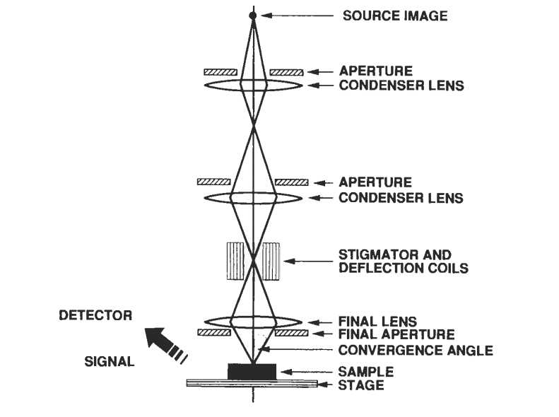
The main features of the instrument are the electron column containing the electron source i.e gun, the magnetic focusing lens, the sample, the vacuum chamber, and the stage region.
- Electrons required for illumination are emitted from an electron source or electron gun that could be thermionic or field emission type.
- The wide-angled electrons are blocked by an aperture and narrow-angled electrons are sent through a condenser lens that focuses the electrons to a tiny spot.
- The electron beam is focused on the sample with the help of an objective lens. Beam scanning is achieved by magnetic coils that help to deflect the beams laterally on the sample so that raster scanning can be done.
- The emitted electrons are detected with the help of an electron detector. The detector signal is amplified by an amplifier and displaced in the display unit.

Sample specification for SEM
- Imaging is done at a high vacuum (< 10-4 pa) and dry environment so a watery sample can not be imaged.
- The sample is required to be conductive ( if not charging issue give background, electrons accumulated in sample giving bright spots in the image.)
- If the non-conductive sample is to be imaged, the thin layer of metals like Gold and iron is to be coated using sputtering.
Applications of scanning electron microscopy
Scanning electron microscopy is most often used to reveal the following information.
- It produces 3D images with a high resolution of thin-films and large depth.
- It identifies quickly the elements present on the sample surface.
- Topographical, morphological, compositional, and crystallographic information about the sample can be obtained.
- Defects in the crystal can be detected.
- Grain structure, grain size, and shape.
Limitations of Scanning electron microscopy
Although it has vital application and advantages, this technique is limited by the following facts.
- It may be destructive in nature.
- Insulating samples need to be coated with a metal.
- Vacuum compatibility is typically required.
Scanning electron microscopy youtube video
What is the main difference between SEM and TEM?
In SEM, the electron beam is passed through the sample, and only emitted electrons and backscattered electrons are collected. But in TEM(Transmission electron microscopy), only transmitted electrons are collected and analyzed.


