Transmission electron microscopy principle, instrumentation, advantages, limitations, and the difference between Scanning electron microscopy and transmission electron microscopy have been discussed in this post. Transmission electron microscopy is one of the imaging microscopic techniques in which a highly energetic electron beam is used to interact with the sample and transmitted as well as the diffracted beam is measured. TEM was first of all developed by Ernst Ruska in the 1930s.
Transmission electron microscopy principle
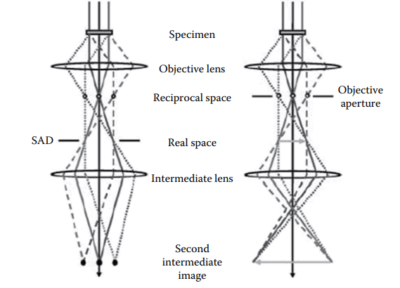
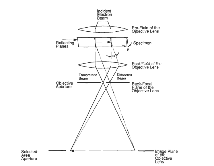
In TEM, a thin solid specimen ( < 200 nm thick) is bombarded in a vacuum with a highly focused, monoenergetic beam of electrons. The beam is of sufficient energy to propagate through the sample. A series of electromagnetic lenses magnify this transmitted electron signal and delivered the signal to a detector.
A typical TEM microscope can be operated in two modes:
- Image mode
- Diffraction mode
Image mode
In this mode, the electron beam is allowed to pass through the sample and transmitted electrons are projected on a camera to get a high-resolution image of a thin sample. There are three primary image modes that are used in conventional TEM, bright field, darkfield, and high-resolution electron microscopy, also known as a phase-contrast mode.
Diffraction mode
In diffraction mode, an electron diffraction pattern originating from the sample is illuminated by the electron beam obtained on the fluorescent screen. The diffraction pattern is entirely equivalent to an x-ray diffraction pattern. A single crystal will produce a spot pattern on the screen, a polycrystal will produce a powder or ring pattern and a glassy or amorphous material will produce a series of diffuse halos.
Transmission electron microscopy instrumentation
The basic elements of TEM are listed below.
- Electron source: Electrons needed for illumination is generated from thermionic or field emission type electron gun.
- Condenser lens: The wide-angled electrons are blocked by an aperture or slit and beam size is reduced by using the first condenser(Electromagnetic type) lens. The second condenser lens focuses the beam to a narrow spot on the sample.
- Objective lens: The electrons that are transmitted from a thin sample are collected by the objective lens. To select the proper mode of operation, an aperture is placed on the back aperture of the objective lens.
- Projective lens: The focused image made by the objective lens is magnified by using a pair of intermediate and projector lenses.
- Detector: The magnified image is projected into an electron-sensitive camera to get an image of the sample.
Advantages of Transmission electron microscopy
- It uses only 60-300kV for the acceleration of electrons.
- It has a much higher magnification than SEM.
- TEM has superior image resolution.
- TEM-EDS provide an excellent spatial resolution of 2-3nm for elemental identification.
Limitations of Transmission electron microscopy
- It has limited depth resolution.
- Sample preparation for TEM is critical. A very thin layer of sample is required.
- It is one of the most expensive imaging techniques.
Scanning electron microscopy vs Transmission electron microscopy
The main differences between the SEM and TEM are listed below:
| Scanning electron microscopy(SEM) | Transmission electron microscopy(TEM) |
| It uses 50-500 KeV | It uses 60-300KeV. |
| Low magnification of the image | It has a much higher magnification |
| It creates an image by detecting reflected or knocked electrons. | It uses transmitted electrons to create an image. |
| SEM provides information on the sample’s surface and its composition. | TEM provides valuable information on the inner structure of the sample such as crystal structure, morphology, stress state information |
| Spatial resolution is limited. | Resolution less than 50 pm. |
| For surface information, like roughness or contamination, it is used | For internal structure, like crystal structure, crystal defects, it is used. |
| SEM provides a 3D image of the surface of the sample. | TEM images are 2D projections of the samples. |
| Sample preparation is not so hard. | The sample must be very thin. |
| The maximum field of view is large for SEM. | TEM users can only image a very small part of the sample. |
| The sample is positioned at the bottom of the electron column. | The sample is located in the middle of the column. |
TEM youtube video
References
- C. R. Brundle, C. K. Evans, Jr., S. Wilson and L. E. Fitzpatrick (eds), Encyclopedia of Materials Characterization: Surfaces, Interfaces, Thin Films, Butxetworch-Heinemann, Reed Publishing (USA) Inc., 1992.