Nanolithography, or nanopatterning having at least one lateral dimension between the size of an individual atom and roughly 100 nm, is the area of nanotechnology concerned with the research and use of the nanofabrication of structures on a nanometer scale. The name “nanolithography” comes from the Greek terms “nanos,” which means “dwarf,” “lithos,” meaning means “rock or stone,” and “graphein,” which means to write. Nanolithography is used in nearly every essential application across many different scientific fields in nanoresearch, such as the nanofabrication of cutting-edge semiconductor integrated circuits (nanocircuitry), nanoelectromechanical systems, and more.
Some of the nanolithography techniques are discussed below:
STM based nanolithography
Scanning Tunneling microscopy (STM) has been applied for the generation of various nanostructures in self-assembled monolayers. STM has much higher spatial resolution and sensitivity than electron beam nanolithography, which is one of the reasons it is a particularly appealing lithographic technique. STM lithography for nanofabrication mostly involves material modifications, deposition, removal, and manipulations.
- Material modification: Several nanopatterns can be produced using scanning tunneling microscopy lithography (STML). The local oxidation of a hydrogen-passivated Si substrate in the air has been studied using STM, and it has been found that the presence of oxygen and the OH group at the tip target contact enhances local oxidation/diffusion. As a result, different nanopatterns can be produced by delivering a bias pulse to the STM tip-sample tunneling junctions.
- Material deposition: STM tips are used as a tiny emission source in STML applications for the direct deposition of metals. Atoms or nanoparticles are moved from the tip to the target surface within the tunneling distance when voltage is applied. Although both positive and negative voltages were used for the deposition, the tip’s negative polarity is typically more stable, has a higher likelihood of transfer, and can produce features with smaller sizes.
- Material removal and etching: The removal of materials from the surface can be accomplished via electron beam-induced thermal decomposition. The electron dose, which is what drives this process, can be managed by varying the emission current and exposure time. Many patterns and pattern sizes can be created by controlled tip scanning. In the presence of chemical solutions, STML can also carry out electrochemical etching of materials. Comparable nanohole production is possible with dry etching. Although the precise mechanism of nanohole production is not fully understood, various contentious theories, including as local heating, electromagnetic, and chemical reductions, have been put forward.
AFM based nanolithography
Both contact mode and tapping mode can be applied during AFM imaging or lithography. The mechanical action of the AFM tip, which is employed as a sharply pointed tool to create fine grooves on sample surfaces, is referred to as direct contacting, writing, or scratching. Although direct scratching creates grooves with high precision, low-quality results are often obtained due to tip wear during the process.
An alternative method involves using scratching to create a mask for the etching process on a soft resist polymer layer, like PMMA or polycarbonate and then using etching to transfer the pattern to the sample surface. Although this approach guarantees less tip damage, it also makes it impossible to accurately align the structures below. Another enhancement being explored is a two-layer mask.
For instance, 50 nm-wide structures were created using a mask coating made of a thin layer of 50–100 m polycarbonate and a film of an easily deformable and fusible metal, like indium or tin.
Dip pen nanolithography
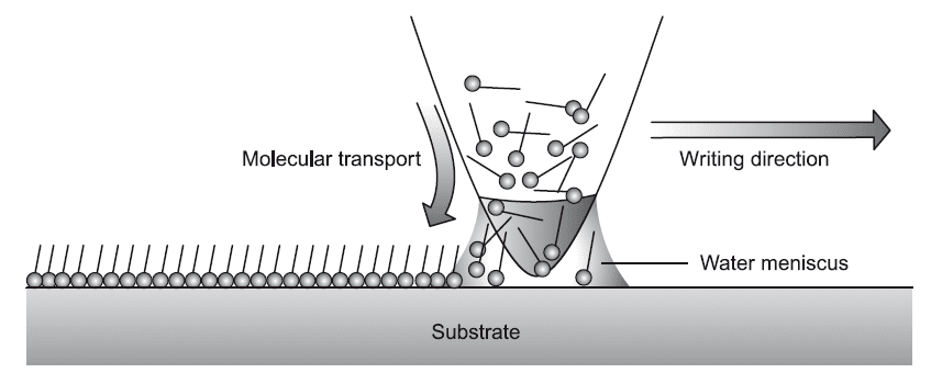
In dip-pen nanolithography (DPN), a surface is in touch with a chemical that has been “inked” onto the tip of an AFM that is operating in the air. Similar to a fountain pen, the ink molecules flow from the tip onto the surface. In a highly humid environment, a drop of water condenses between the tip and the surface, acting as a bridge for molecules that adsorb to the tip surface to migrate to the substrate surface for pattern creation. It is possible to dip the tip into a solution containing the molecules in low concentrations, dry it (for instance, by blowing it dry with compressed difluoroethane), and then ink it. With this approach, line widths as small as 12 nm and spatial resolutions as small as 5 nm have been obtained.
Inorganic, organic, biomolecules, and conducting polymers have all been deposited via dip-pen nanolithography on a variety of surfaces, including metals, semiconductors, and functional surfaces. Temperature, humidity, tip-substrate contact force, writing speed, and the physiochemical properties of the link and substrate are some of the factors that affect successful DPN.
One of the major applications of dip pen nanolithography is patterning octadecanethiol self-assembled monolayers on gold surfaces.
E-Beam Nanolithography
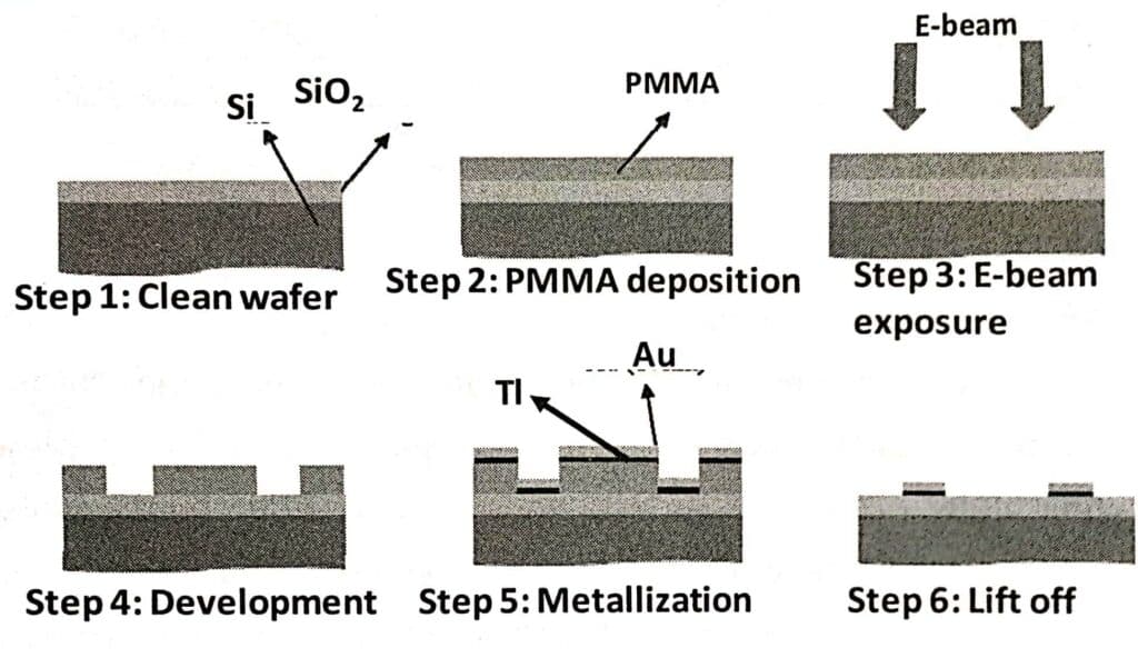
E-beam nanolithography, also known as electron beam nanolithography, is a nanopatterning process that uses electron beams to write sub-10 nm nanopatterns. A polymer resist is initially applied to the clean substrate, either a positive resist (like polymethyl methacrylate, which becomes more soluble when exposed to an electron beam) or a negative resist (like hydrogen silsesquioxane, which becomes less soluble when exposed to an electron beam). The evenly polymer-coated substrate is then put into the electron microscope, where a pattern is created by shining the electron beam at a specific location.
After being exposed to an e-beam, the material is developed by dipping it into a solution that dissolves the chosen portion of the resist. After the resist has been exposed, the materials to be patterned are sputtered on it such that they directly deposit on the substrate surface. Lastly, the metal that was deposited on top of the polymer is removed from the substrate surface along with the polymer by exposing it to the solvent that dissolves the polymer. As a result, the material’s surface is precisely coated with a well-designed pattern.
Ion beam Nanolithography
Similar to electron beam lithography, ion beam nanolithography employs charged ions rather than electrons. Because they are heavier than electrons, ions have less path bending and diffract less. Ion-beam nanolithography, as opposed to E-beam lithography, aids in the creation of higher-resolution patterns as a result of these characteristics.
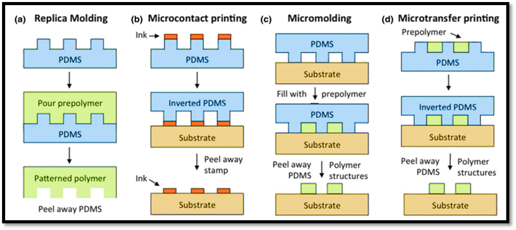
Nanoimprint lithography and soft lithography
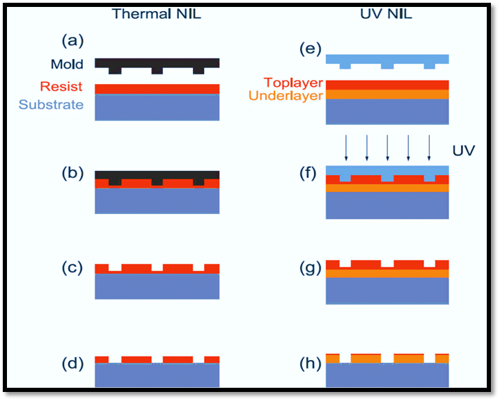
Nanoimprint lithography creates patterns on soft polymers such as liquid PMMA by using a hard mold (quartz or silica). Lithographic methods like electron beam lithography are used to create the nanopattern on the mold. The mold is then brought into contact with the melted polymer once the polymer has first been heated to that point. The temperature is lowered when the polymer has filled the mold’s structure so that it can solidify. In order to solidify polymers, they can also undergo UV or heat treatment during processing. The polymer is then freed from the mold, and a nanoimprint is produced.
A soft polymer stamp is used in the relatively straightforward approach of soft lithography to transfer a pattern (surface coated with molecules, such as ink). The creation of the polymer pattern and the transfer of the pattern to the substrate are the two fundamental phases. A soft elastomeric mold (polydimethylsiloxane) is dipped in the solution of the molecule to be patterned and brought into contact with the substrate in pattern transfer, which is analogous to rubber stamping. Using a polydimethylsiloxane (PDMS) stamp to transfer thiols onto a gold surface is one excellent example.